MCU PCB Design
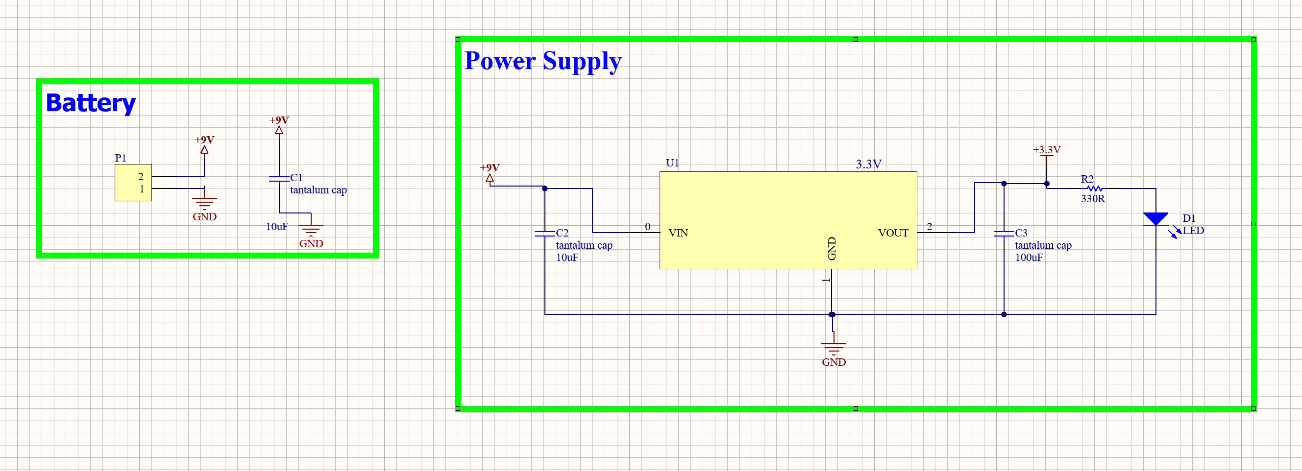
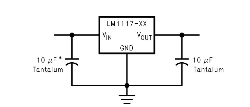
The entire design process was carried out using Altium Designer. The initial step involved drafting the schematics for both the power supply and the microcontroller unit. The power supply schematic was created first and includes a battery and a voltage regulator section. The battery provides a 9V input to the system, which is regulated down to 3.3V by the voltage regulator. The regulator was designed using a custom component (U1), which models the Texas Instruments LM1117 low-dropout voltage regulator. Following Texas Instruments' system examples, the design incorporates a 10 µF and a 100 µF tantalum capacitor to ensure power regulation. The 100 µF capacitor was specifically chosen to stabilize the output voltage.
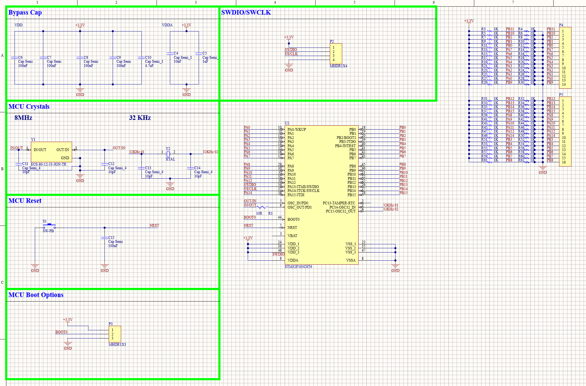
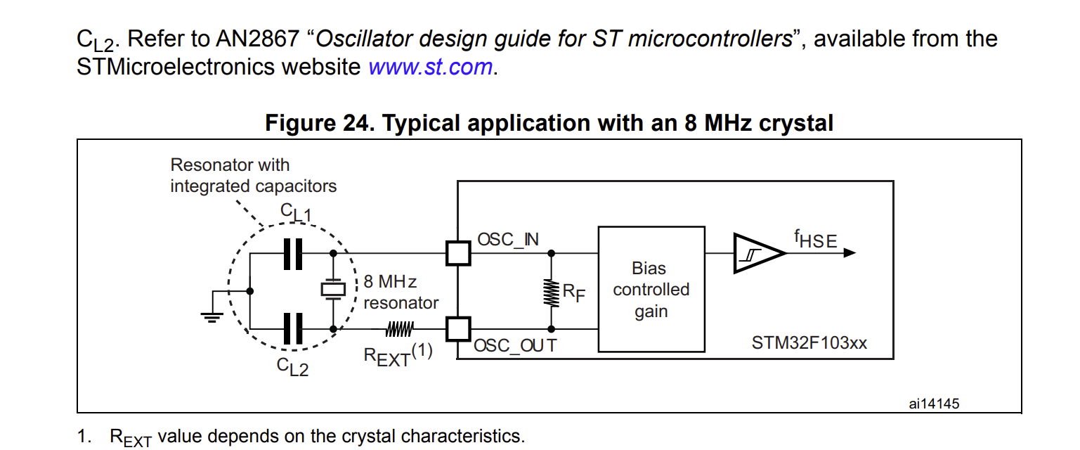
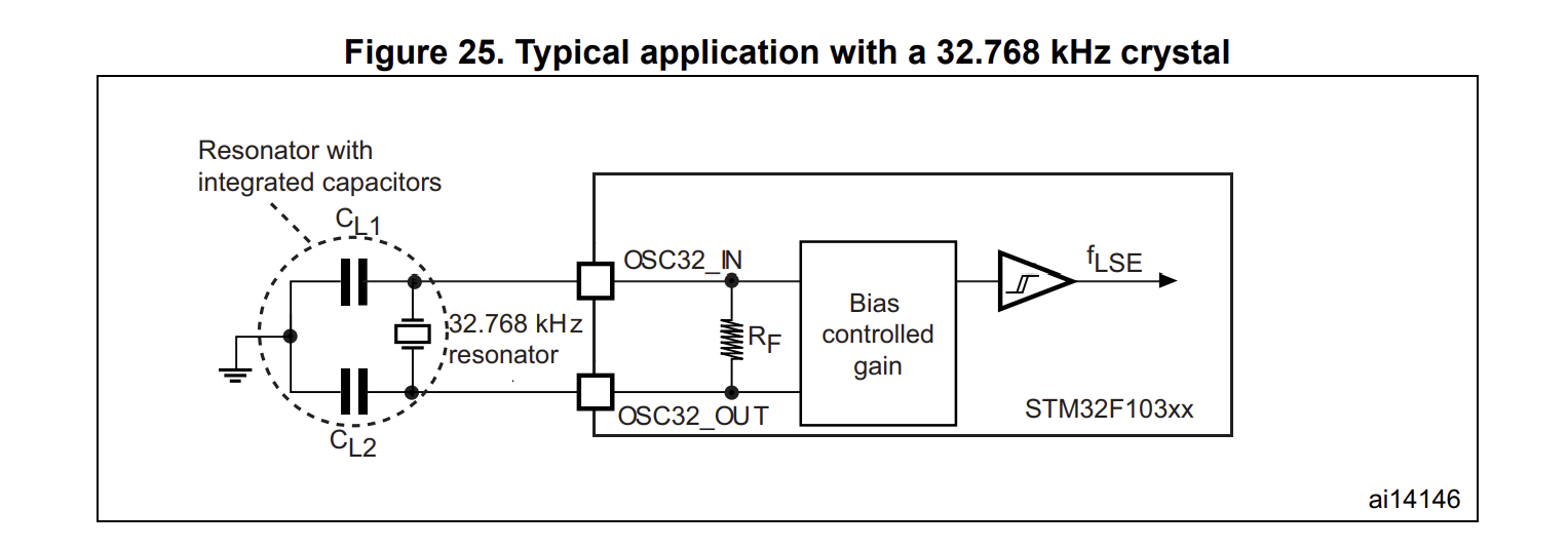
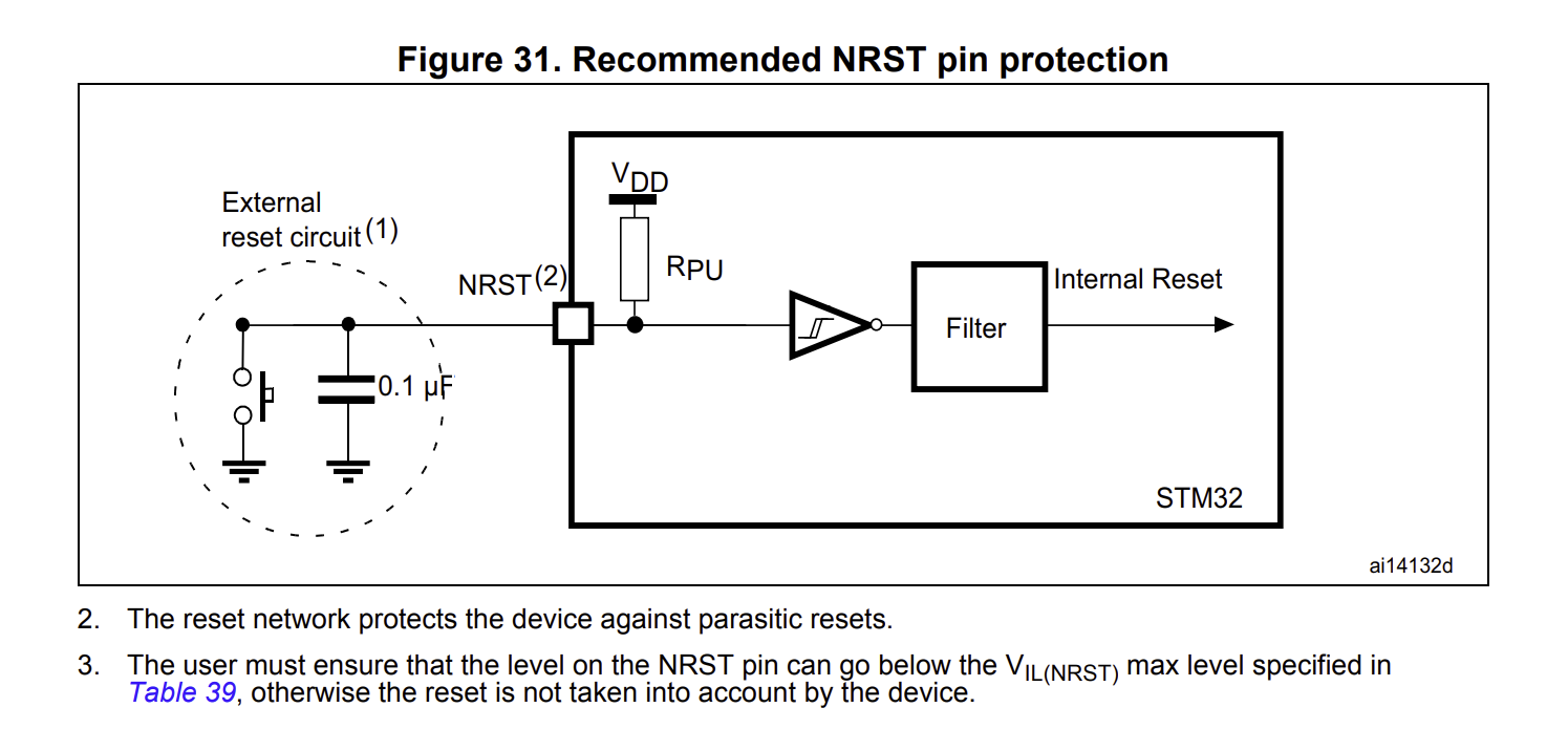
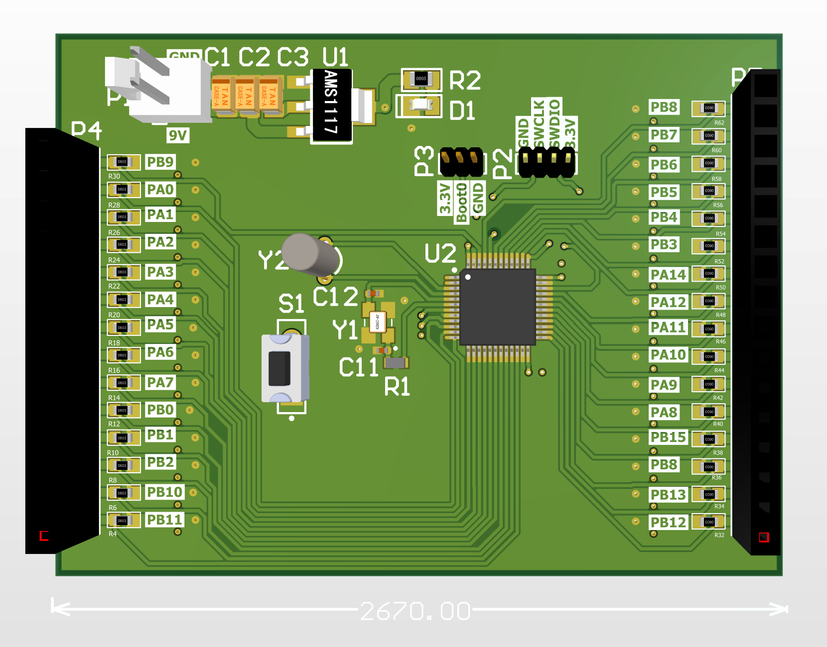
The microcontroller schematic consists of sections for bypass capacitors, SWDIO/SWCLK pins, 8 MHz and 32 kHz crystals, reset and boot options, and pin header connections. The complete schematic, including all components, is shown below, alongside the documentation used as references. In my microcontroller PCB design, bypass capacitors stabilize the power supply by filtering out noise, while the SWDIO/SWCLK pins enable programming and debugging via the Serial Wire Debug interface. The 8 MHz and 32 kHz crystals provide stable clock signals for core processing and real-time clock functions, respectively. Reset and boot options allow for system resets and configurable boot modes, and pin headers provide easy access to the MCU’s I/O and communication interfaces for external device connections.
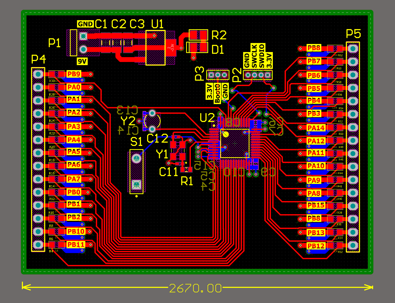
Below, the final PCB layout before the polygon pour is shown, along with a 3D view of the board. The 3D models of the components were developed using Altium Designer.
Resources